
For forty years, the secret language that lets software talk to hardware was owned by a handful of c 2026-7-9 04:35:25 Author: hackernoon.com(查看原文) 阅读量:12 收藏
For forty years, the secret language that lets software talk to hardware was owned by a handful of companies. Then a free alternative escaped the lab—and turned chip design into a matter of statecraft.
There is a sentence that security researchers, hardware startups, and the governments of at least three continents have all, in their own way, come to believe: you can put a company on a blacklist, but you cannot put a language on one.
That single insight is quietly rewiring the most concentrated industry on Earth. For more than four decades, the foundational vocabulary of computing — the instruction set architecture, or ISA, that determines how a piece of software actually speaks to the silicon beneath it — has been guarded like a crown jewel. In PCs, laptops, and servers, the proprietary x86 architecture built by Intel and AMD has reigned almost unchallenged. In phones and embedded gadgets, the British-born ARM architecture has been nearly as dominant. If you wanted to design your own processor, you paid millions in licensing fees, signed thick stacks of non-disclosure agreements, and accepted black-box silicon you could neither fully audit for hidden flaws nor bend to an unusual purpose.
That world is ending. Driven by the spread of open standards, the maturing of free chip-design software, and a global anxiety about who controls the supply chain, open-source silicon has vaulted from an academic daydream into a commercial reality. Processors designed collaboratively, in the open, are now booting Linux, shipping inside consumer laptops, rendering 3D graphics, and locking down the firmware in enterprise data centers.
This is the story of how that happened — and of why a royalty-free dictionary for talking to a chip became one of the most contested objects in twenty-first-century geopolitics.
Three things people mean when they say "open"
Before going further, it helps to untangle a knot that casual coverage almost always leaves tied. "Open" in silicon means at least three different things, stacked on top of one another.
The first is an open instruction set. The ISA is the vocabulary of commands a processor understands — add these two numbers, fetch this from memory, jump to that instruction. The catalyst for everything that follows is RISC-V (pronounced "risk-five"), a free and open ISA born in 2010 as a research project at the University of California, Berkeley, under the eye of computing pioneer David Patterson. RISC-V is an open standard, much like PDF or Ethernet: a universal, royalty-free dictionary describing how software talks to hardware. It says nothing about how the hardware must be built. Anyone — a teenager or a hyperscale cloud provider — can download the spec and build a chip that speaks RISC-V without paying a cent.
The second is an open-source implementation. This is the actual circuit blueprint — the register-transfer-level (RTL) code, written in hardware languages like Verilog, Chisel, or SpinalHDL, that specifies the chip itself. Because the ISA is free, designers can choose: keep their physical design proprietary, or release the RTL to the public under permissive licenses like Apache 2.0 or MIT. Both happen. Alibaba's XuanTie cores, for instance, implement the open RISC-V ISA but open-source only some of their designs.
The third is open-source software: the compilers (GCC, LLVM), the operating systems (Linux, FreeBSD), and — crucially, as we'll see, for graphics — the drivers.
A chip can be open at one layer and sealed at the others. This three-layer model is the analytical spine of the entire field, and missing it is how pundits end up confused.
 The RISC-V mark. Image: RISC-V Foundation / Wikimedia Commons (public domain).
Why RISC-V won the open-ISA race is a story of good engineering. Its design is modular: a small mandatory base of integer instructions, plus optional extensions — M for multiply, A for atomics, F and D for floating point, C for compressed instructions, V for vectors. The combination nicknamed "RV64GC" became the de facto baseline for Linux-capable chips. This lets a designer add only what an application needs, and — impossible with ARM or x86 — add custom instructions of their own. To keep that freedom from fracturing into a thousand incompatible dialects, the governance body, RISC-V International, ratifies "profiles" (such as RVA23, ratified in 2024) that bundle mandatory features together.
The mere existence of a credible free option has bent the older players. The Power ISA, once a closed IBM fortress used in supercomputers, faced such pressure from RISC-V's rising mindshare that the OpenPOWER Foundation pivoted to a far more open model, granting royalty-free access to build custom implementations. But RISC-V's deeper victory was platform standardization — nailing down how firmware and power-management interfaces work so that a generic copy of Debian Linux can boot across wildly different RISC-V hardware.
|
ISA |
Ownership |
Where it rules |
Notes |
|---|---|---|---|
|
x86 |
Intel and AMD only |
PCs and servers |
Deepest software ecosystem |
|
ARM |
Licensed by Arm Holdings (SoftBank) |
Mobile, Apple Silicon, Amazon Graviton |
Rich vendor ecosystem, hefty license fees |
|
RISC-V |
Open, royalty-free; Switzerland-based RISC-V International |
Embedded, growing into servers and AI |
The only mainstream ISA you can extend with your own instructions |
|
OpenPOWER / OpenSPARC |
Freed by IBM and Sun |
Legacy supercomputing, niche |
Technically open, but lacking RISC-V's momentum |
The vanguard: open chips that can keep up
For years, open processors lived at the bottom of the food chain — tiny educational cores, motor controllers, the brains of a cheap IoT gadget. The assumption was that serious, high-performance design required the secrecy and capital of an Intel. A new generation of superscalar, out-of-order open processors is dismantling that assumption.
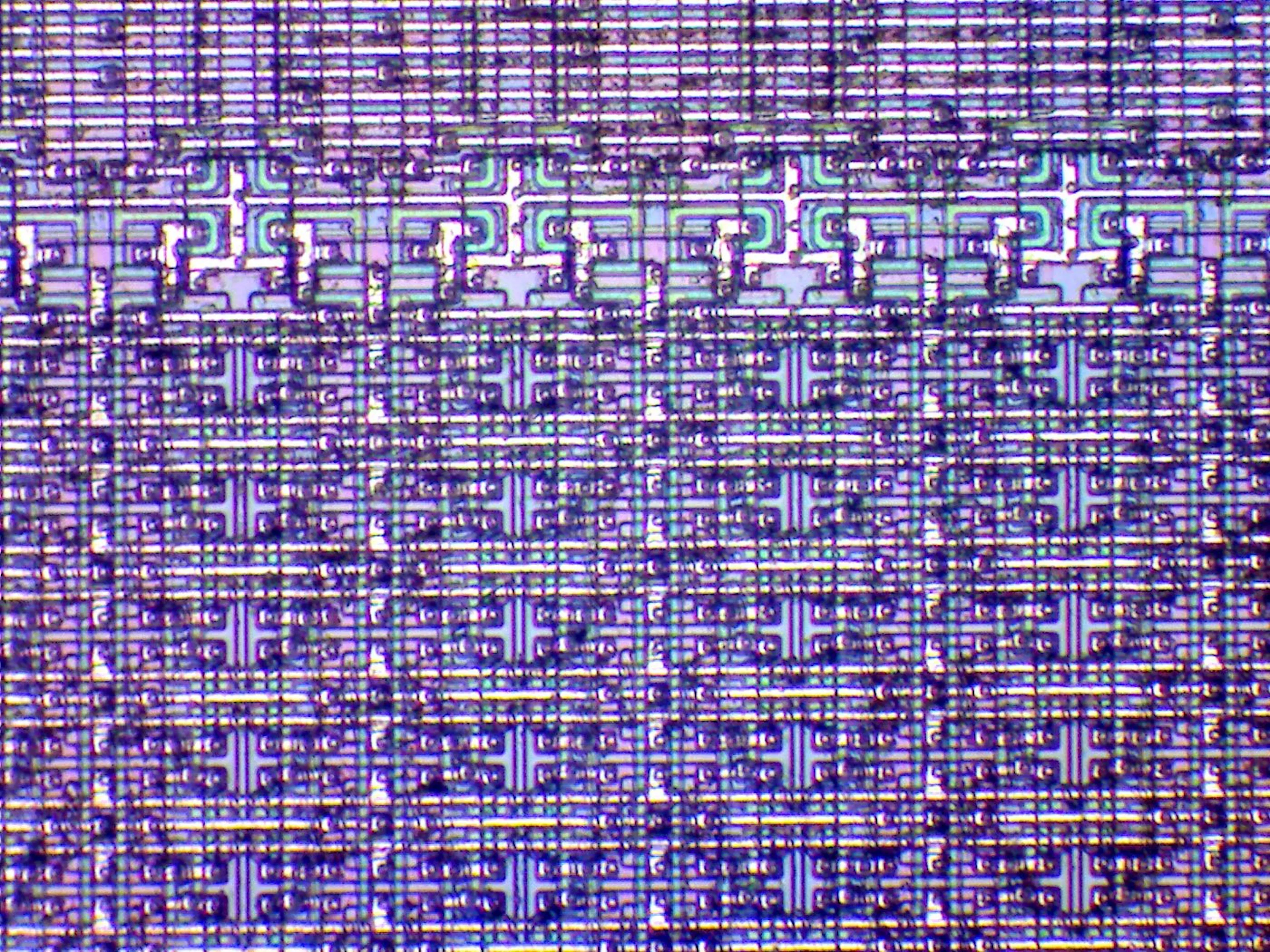
XiangShan: an open chip aimed at the data center
The most ambitious of these efforts comes out of the Chinese Academy of Sciences, developed at the Beijing Institute of Open Source Chip (BOSC). The XiangShan project, written in the Chisel hardware language, uses an "agile" design style — tweak the model, recompile the blueprint, measure again — borrowed straight from how modern software teams work.
XiangShan has marched through three generations, each named after a Chinese lake. Yanqi Lake (first generation) taped out on a 28-nanometer process in July 2021 at 1.3 GHz, with an 11-stage out-of-order pipeline. Nanhu (second generation) hit 2 GHz on a 14nm process and widened the chip's front end and memory system. But the third generation, Kunminghu, is the leap: a heavyweight design built for advanced sub-10nm nodes at 3 GHz, with a 6-wide decode-and-dispatch engine, a 224-entry integer register file, sophisticated branch prediction, and four vector units compliant with the modern RVV 1.0 standard.
How good is it, really? Here the honest picture matters. According to Prof. Yungang Bao of the Institute of Computing Technology, presenting at the RISC-V Summit Europe in 2025, the Kunminghu V2 generation reaches roughly 15 points per gigahertz on the SPEC CPU2006 benchmark — "with comprehensive performance close to that of ARM's Neoverse N2," a respectable data-center core. Chinese state media has cited a slightly rosier 16.5 points/GHz, drawn from physical test chips made by commercial partner SpacemiT, and described it as reaching "internationally advanced levels." The number to remember is this: an openly published chip design now lands in the same competitive neighborhood as ARM's server-class cores. That alone proves the open-source community can shoulder the staggering verification burden — differential testing, formal methods, nightly regressions — that modern CPUs demand.
Ascalon: Jim Keller bets on open
Then there is Tenstorrent, the company led by Jim Keller, the architect behind landmark designs at AMD, Apple, and Tesla. Its Ascalon family of RISC-V cores is built explicitly for the AI era. Compliant with the RVA23 profile, the top-end Ascalon X is a 64-bit out-of-order core capable of clocking past 2.5 GHz on a cutting-edge 4nm process, with an enormous 8-wide decode engine and dual 256-bit vector units tuned for the dense matrix math of large language models. Independent analysis of the design suggests a ferociously fast scalar core — executing simple integer operations in a fraction of a cycle — and explicit support for the low-precision number formats (BF16, FP16) that AI inference lives on.
Tenstorrent's wider bet is on chiplets: instead of one giant monolithic die, it builds Ascalon cores as modular blocks that snap together over standardized fabrics, letting other vendors mix Tenstorrent's compute with their own accelerators. The pitch is the elimination of vendor lock-in at the silicon layer itself.
One anecdote captures the cultural difference better than any benchmark. Tenstorrent's chief operating officer has recounted that when the company needed BF16 support, ARM quoted a multi-year internal process to consider adding it — while on RISC-V, a partner "just put it in there." As he put it: "There is no restriction. It is freedom."
From simulation to something you can buy
The proof of any chip is in shipping it. SOPHGO's SG2042 packs 64 RISC-V cores (the XuanTie C920, from Alibaba's T-Head division) at 2 GHz, backed by 64 MB of cache and four DDR4 memory channels. Hardware maker Milk-V dropped it onto the "Pioneer," a standard mATX motherboard with PCIe slots for ordinary AMD or Nvidia graphics cards, letting developers build a native RISC-V desktop and compile code without crawling through emulation.
But the honesty test comes from independent benchmarking, and it is sobering. Academic researchers at EPCC, led by Nick Brown, found that mainstream x86 server chips outperform the SG2042 "by between four and eight times for multi-threaded workloads." The technology analysts at Chips and Cheese pegged the SG2042 as roughly comparable to Amazon's first-generation Graviton ARM chip — about five years off the leading edge. The newer SG2044 narrows the gap, but on single-core work an AMD EPYC still delivers about twice the performance and an Intel Skylake about three times.
The trajectory points up and to the right — but the leaders have not been caught.
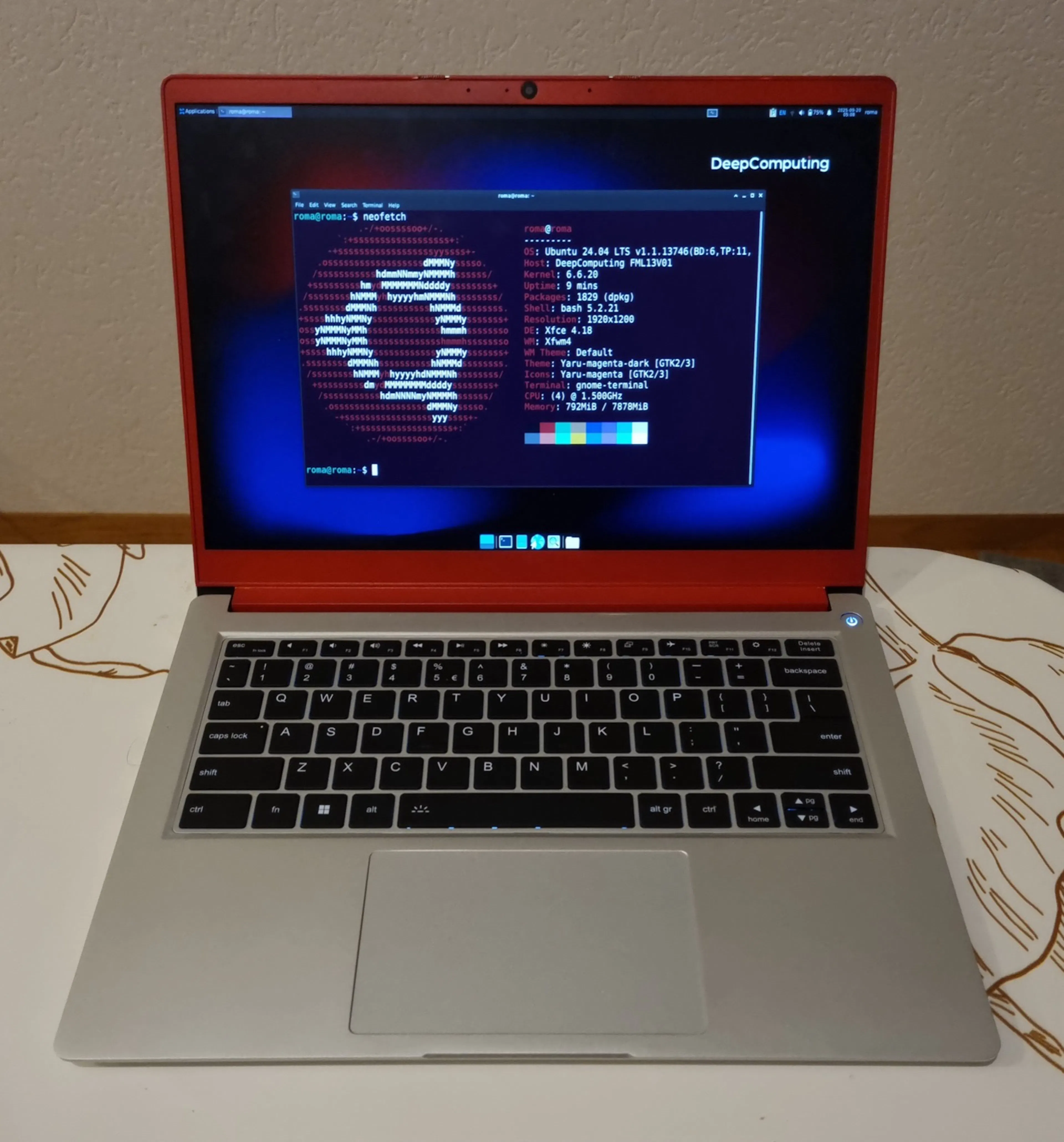
You can hold the results in your hands. China's SpacemiT sells the octa-core K1 chip at the heart of the MuseBook, a roughly $300 RISC-V laptop aimed squarely at developers running Debian or Ubuntu. DeepComputing built a RISC-V mainboard for the modular Framework Laptop 13 — the first non-x86 board for that machine — though Framework is refreshingly candid that it is "focused primarily on enabling developers, tinkerers, and hobbyists," not winning benchmark wars. For the data center, SpacemiT's VitalStone V100, on a 12nm process, fuses 40 of its in-house X100 cores with 6 high-performance XiangShan Kunminghu cores into a 64-core server chip with the virtualization and I/O features enterprise infrastructure demands.
|
Tier |
Representative part |
Versus the proprietary leaders |
|---|---|---|
|
Microcontroller |
Espressif ESP32-C3/C6 (RISC-V) |
Competitive on cost and efficiency |
|
Single-board / edge |
SpacemiT K1 (Banana Pi BPI-F3) |
Below ARM Cortex-A76 class |
|
Server (shipping) |
SOPHGO SG2042 / SG2044 |
~Graviton 1; two to eight times behind current x86 |
|
Server (on paper) |
SiFive P870, XuanTie C930, Tenstorrent Ascalon |
Claims near ARM/AMD; unproven in market |
|
Open-RTL high-perf |
XiangShan Kunminghu |
~ARM Neoverse N2 (per its developers) |
The quiet empire: chips you'll never see
The headlines chase laptops and servers, but the real volume of silicon hides in the unglamorous middle of the world — storage controllers, industrial state machines, motor controls, IoT endpoints. Here, where a per-chip ARM licensing fee can erase a product's entire margin, open silicon has all but taken over.
Western Digital realized early that paying to license an ISA for the controllers inside its drives — when it ships over a billion cores a year — made no economic sense. So it designed and open-sourced its SweRV family of RISC-V cores. The flagship SweRV EH1 hit a brisk 5.0 CoreMarks per megahertz, outrunning comparable proprietary cores, and Western Digital handed commercial stewardship to the CHIPS Alliance, catalyzing adoption across the storage industry.
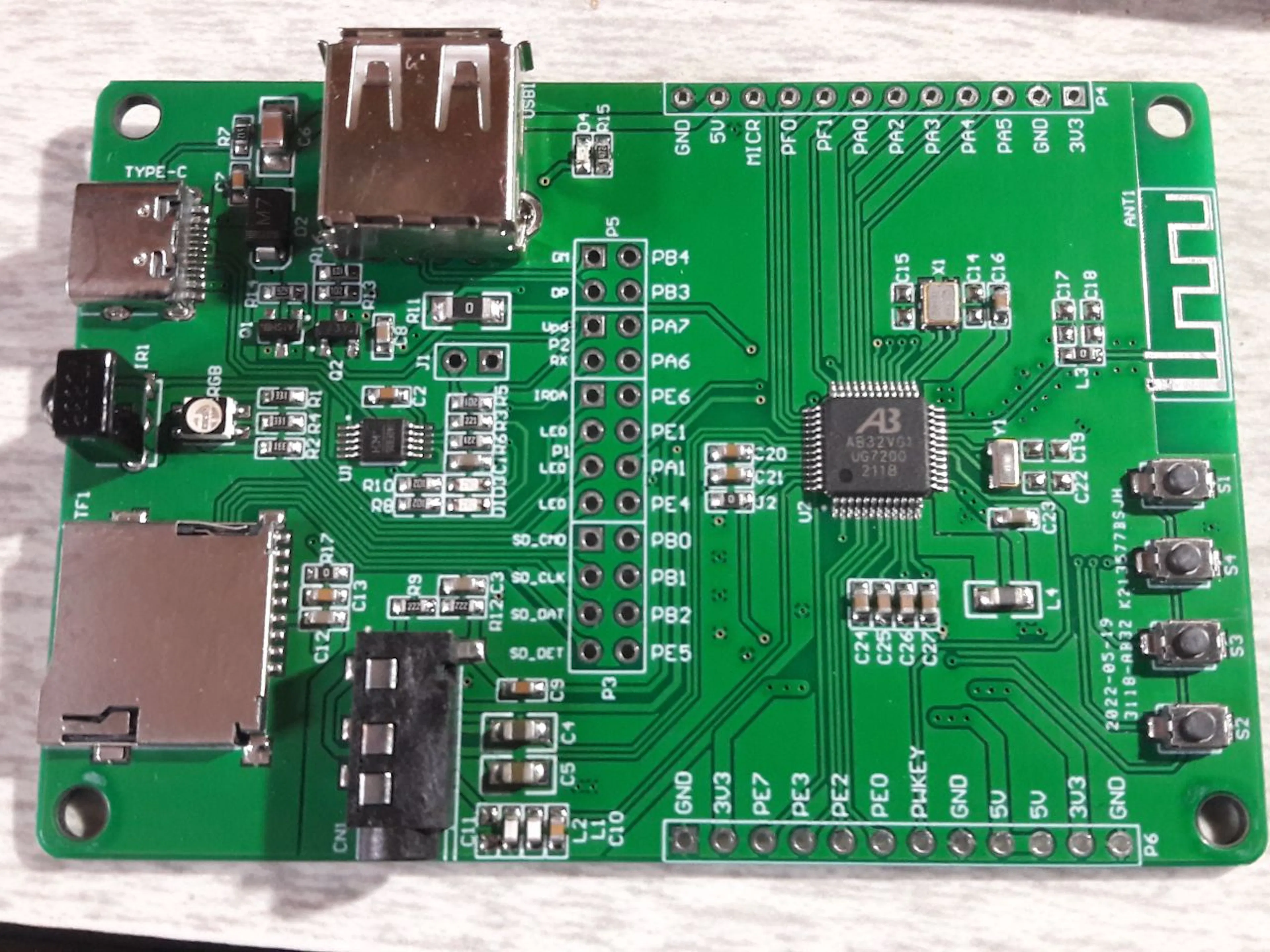
The OpenHW Group, under the Eclipse Foundation, curates the industrial-grade CORE-V family: the Linux-capable CVA6 (descended from ETH Zürich's Ariane core), down to the featherweight CVE2 built for maximum energy efficiency. And lowRISC's tiny, formally verified Ibex core has become the quiet workhorse of hardware security — it's the brain inside Google's OpenTitan root-of-trust, of which more shortly.
In sheer numbers, this is where the revolution has already, decisively won. The cores are everywhere; you simply never see them.
The graphics chasm
If open CPUs are a confident teenager, open GPUs are a toddler — and the gap is instructive. Graphics chips are vastly harder to open-source, for two reasons: their internal architectures are enormously more complex, coordinating thousands of parallel threads, and the surrounding software stack — drivers, shader compilers, graphics APIs — is a mountain unto itself, ringed by patent thickets.
The history is short and humbling. MIAOW (Wisconsin, 2015) cloned a slice of an AMD GPU but produced no graphics output and, by copying AMD's instruction set, gained no independent legal footing. Nyuzi (Jeff Bush) is a fully working software-rendering GPU — but on a custom ISA, achieving only about a quarter of a commercial embedded GPU's performance per watt.
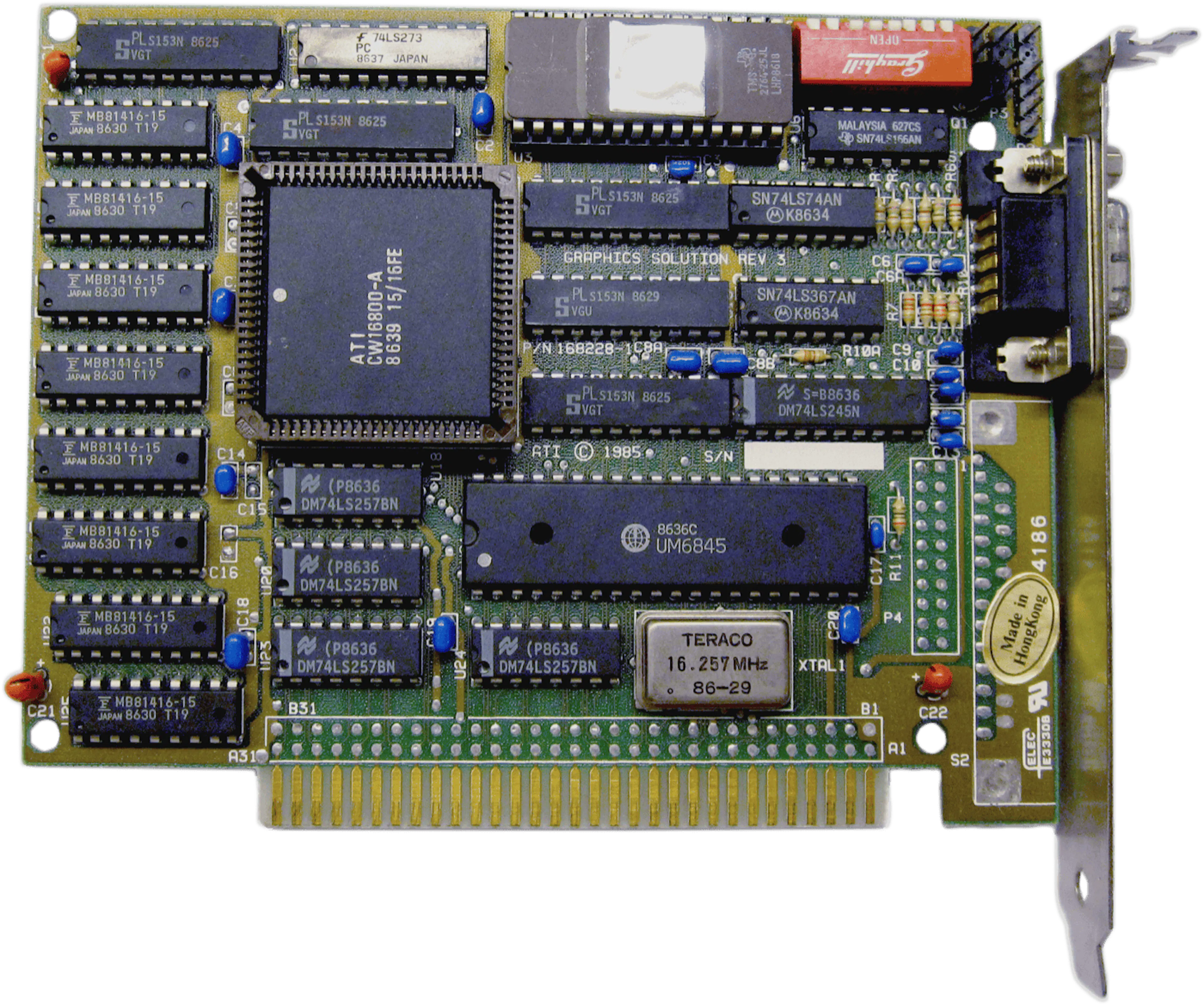
The field's standard-bearer is Vortex, developed at Georgia Tech under PhD student Blaise Tine. Its key move is elegant: instead of inventing a wholly separate, proprietary GPU instruction set the way commercial vendors do, Vortex extends the existing RISC-V ISA with a minimal set of additions to support the SIMT ("single instruction, multiple threads") execution model GPUs rely on. By reusing the RISC-V base, it keeps the existing toolchain usable and sidesteps the crushing labor of building a compiler stack from scratch. Vortex is open all the way down: the RTL, a cycle-accurate model, an LLVM compiler, and an OpenCL runtime.
The engineering has accelerated fast. A re-architected front end with a multi-warp scheduler — interleaving up to 16 warps to hide memory latency — drove pipeline utilization from a sparse 13.2% to a dense 64.3%, a roughly fourfold speedup. A June 2026 release added a full fixed-function 3D graphics pipeline, a Vulkan driver, and tensor-core features. As Tine put it: "Before RISC-V, building full-stack GPU hardware would have been an insurmountable task that only large companies would have had the resources to do."
But the honest verdict is non-negotiable: Vortex is the most capable openly synthesizable GPU in existence and an invaluable research and teaching platform — it has even flown in safety-critical space-systems research — but it is not, and does not pretend to be, a competitor to Nvidia or AMD. There is no open-source GPU today that approaches commercial graphics performance.
Others probe different angles. The RV64X project proposes a fully fused CPU-GPU, treating the graphics unit as a coprocessor bolted directly onto a RISC-V core, with native data types for matrices, pixels, and texels — aimed at low-power industrial displays, robots, and kiosks. The Libre-SOC project, built on the open Power ISA, pursues a clever trick called Scalable Vector Prefixing (SVP64): rather than adding thousands of new vector opcodes the way Intel's AVX-512 does, it simply prepends a prefix to ordinary scalar instructions, turning the pipeline into a hardware-level for-loop. And Kazan, written in the memory-safe Rust language, is a software Vulkan implementation that can render 3D on hardware with no GPU at all — a fallback for systems where die area or licensing forbids dedicated graphics.
Tellingly, the most important open-GPU work today may be in software: the Mesa drivers that already power AMD and Intel graphics on Linux. Commercial chipmakers, meanwhile, take the pragmatic path — SpacemiT's K3 pairs open RISC-V compute cores with a proprietary, Linux-ready Imagination GPU, because a working windowing system today beats a pure-open one tomorrow.
The tensor frontier
Every era of computing has its defining workload, and this one has a shape: the matrix multiply. Training and running a large language model is, at bottom, an ocean of linear algebra — multiplying grids of numbers by other grids of numbers, billions of times a second. A general-purpose CPU is hopeless at this. Even a GPU, built for the parallel firehose of graphics, spends much of its energy shuttling data rather than doing the math. So the industry did what it always does when a workload becomes valuable enough to justify it: it built a machine that does one thing. The AI accelerator — call it an NPU, a TPU, a tensor engine, an ASIC — is silicon stripped down to the single operation that matters, the multiply-and-accumulate, replicated tens of thousands of times.
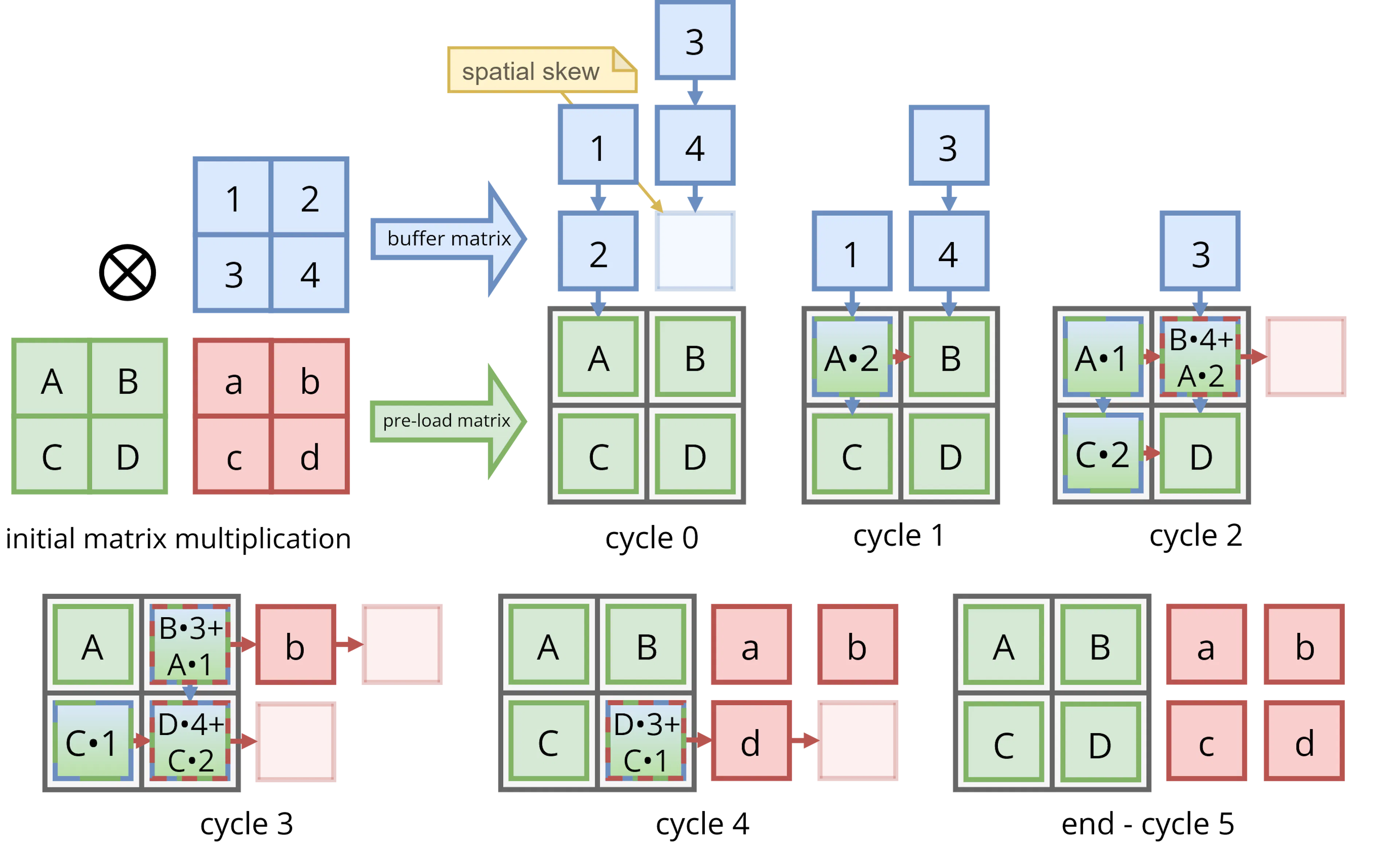
The canonical design is older than the personal computer. In 1978, H.T. Kung and Charles Leiserson described the systolic array — a grid of tiny processing elements through which data is pumped rhythmically, the name borrowed from systole, the contraction of a heart. Numbers stream in from the edges; each cell multiplies, adds, and hands the running total to its neighbor, so a full matrix multiplication ripples across the array with almost no trips back to slow memory. Google's first Tensor Processing Unit, unveiled in 2017, was in essence one enormous systolic array: a 256-by-256 grid of 65,536 multipliers running at 700 MHz. It is also the perfect emblem of the problem this chapter confronts. The TPU is one of the most influential chip designs of the century, and Google has never released a line of its blueprint. You can rent it. You cannot read it.
This is the frontier where the open-silicon story turns at once most thrilling and most humbling — because the AI accelerator is simultaneously the richest prize in the industry and the single hardest place for "open" to win. It is also where the three-layer distinction from the start of this piece — open ISA, open implementation, open software — fractures most revealingly.
Teaching an open chip to multiply
RISC-V's structural advantage is that it can grow toward the workload. The vector extension RVV 1.0, ratified in 2021, gave the ISA the wide data-parallel muscle that AI math demands. But a vector unit is not quite a matrix engine, and here the open world is caught mid-argument: no RISC-V matrix extension has yet been ratified. Two rival proposals are circling the same problem. One, the Integrated Matrix Extension, folds matrix operations into the existing vector registers; the other, the Attached Matrix Extension — pushed hardest by Alibaba's T-Head division — gives the matrix unit its own dedicated registers. Tellingly, T-Head published its matrix-extension specification openly, under an Apache license on GitHub, even as the XuanTie cores that implement it stay proprietary. The vocabulary is being written in the open; the chips that speak it are not.
That pattern repeats across a whole wave of RISC-V AI vendors. SiFive's Intelligence family — the X280, X390, and the matrix-equipped XM series — wraps vector and matrix engines around RISC-V cores and sells them as licensable IP. Barcelona's Semidynamics fuses CPU, vector, and tensor units into a single coherent block aimed squarely at running models like Llama. Andes and others offer their own variants. Every one of them implements the open ISA; every one of them keeps its actual circuit design locked. This is the article's three-layer model in miniature — an open vocabulary wrapped around a closed chip — and in AI silicon it is overwhelmingly the norm.
The open-hardware vanguard
The accelerators whose blueprints you can genuinely download live, almost entirely, in universities. NVIDIA itself seeded the field: in 2017 it open-sourced NVDLA, the NVIDIA Deep Learning Accelerator — a configurable convolution engine with real, synthesizable Verilog and a full testbench, fabricated inside its own Jetson Xavier robotics chips. But NVIDIA lost interest, and the repository has barely moved since 2019 — an open design left to freeze in place.
The livelier work is academic. Berkeley's Gemmini is not a chip but a generator: a program that emits a systolic array of whatever dimensions you specify, bolts it onto a RISC-V core, and has been carried all the way to fabricated test chips on TSMC's 16nm and Intel's 22nm processes. The most prolific record of all belongs to the PULP platform, out of ETH Zürich and the University of Bologna, whose openly licensed RTL has produced a small parade of fabricated AI SoCs — among them Occamy, a dual-chiplet design that even reaches for the exotic HBM memory of commercial accelerators. Columbia's ESP stitches such blocks — NVDLA included — into complete open systems-on-chip. And Google, entirely separately from its secret TPUs, has open-sourced small machine-learning cores like Kelvin and the CFU Playground for cramming neural nets onto tiny FPGAs.
The tell is that every one of these is an edge or research part. They run on mature process nodes, lean on modest on-chip memory, and measure their throughput in TOPS, not petaFLOPS. The open-hardware AI accelerator is real, fabricated, and genuinely useful — at the small end of the world.
Tenstorrent and the meaning of "open"
The most commercially serious bid to build an open alternative to NVIDIA belongs, once again, to Jim Keller's Tenstorrent. Its accelerators — Grayskull, then Wormhole, now the 6-nanometer Blackhole — are not GPUs. Each is a grid of "Tensix" tiles, and, in a fitting irony, every tile is orchestrated by a little cluster of RISC-V cores. A Blackhole card shipping in 2025 fields roughly 120 of these tiles and on the order of 664 trillion FP8 operations per second, for under a thousand dollars.
But Blackhole is the sharpest test in this entire field of what "open" is permitted to mean. Tenstorrent's software is genuinely, fully open: tt-metal, its low-level programming stack and direct answer to NVIDIA's CUDA, is Apache-licensed on GitHub, and a developer owns every layer of the card above the Verilog. The Verilog itself, however, is not public — the RTL is shared only with customers who license the IP under contract. Keller's argument is that this is simply a more honest kind of openness: not a public blueprint, but a guarantee that "you know what you're getting," standards and inspectable software in place of a black box. Whether that counts as open hardware is a real and unresolved dispute — and it lands exactly on the three-layer seam. Tenstorrent is open at the software layer, open at the ISA, and closed at the RTL.
One lineage is going all the way. Esperanto Technologies built perhaps the purest expression of the RISC-V AI dream: the ET-SoC-1, a single 7-nanometer chip packing 1,092 RISC-V cores and delivering better than 100 trillion operations a second inside a 20-watt envelope. The company could not make the economics work and wound down its silicon business in 2025. But in a coda worthy of the Efabless story, a startup called Ainekko acquired Esperanto's intellectual property that November with the express aim of open-sourcing it — releasing the simulator, drivers, and firmware first, with the RTL to follow. A commercial AI chip that failed in the market may yet find its afterlife as open hardware.
|
Layer |
What it is |
Open examples |
Still closed |
|---|---|---|---|
|
ISA |
The instruction vocabulary |
RISC-V vector (RVV); T-Head's Apache-licensed matrix spec |
The ISA is the one layer nearly everyone now shares |
|
RTL (the chip) |
The actual circuit blueprint |
Gemmini, NVDLA, PULP/Occamy, ESP, Kelvin |
SiFive, Semidynamics, Tenstorrent, every frontier trainer, Google's TPU |
|
Software |
Compilers and runtimes |
Triton, MLIR / OpenXLA, Apache TVM, tt-metal |
CUDA, cuDNN |
Esperanto's IP is now being open-sourced by its acquirer, Ainekko.
The two walls
Even a flawless open accelerator would run headlong into two walls that have nothing to do with the instruction set.
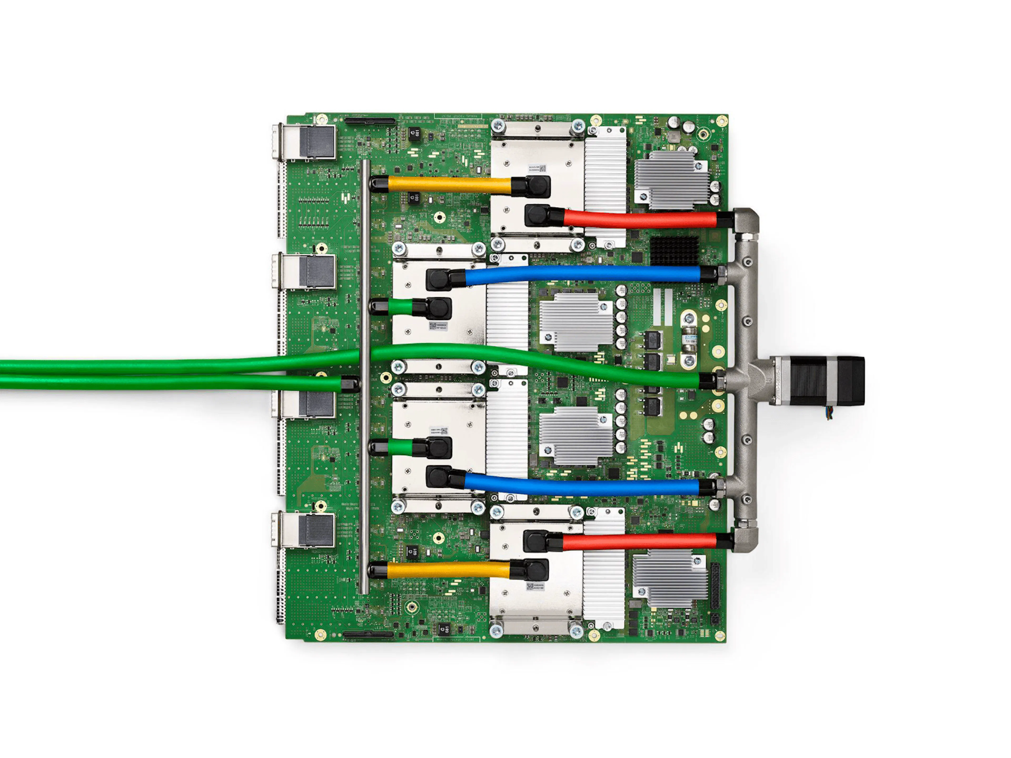
The first is software — the true NVIDIA moat. CUDA turned twenty in 2026; it was unprofitable for most of its first decade and cost billions to build, and its real defense is not the language but the mountain of libraries and the thousands of framework operators piled on top of it. An accelerator no one can program is worthless, which is why every open project in this chapter lives or dies by its compiler. The counteroffensive is itself a stack of open software — OpenAI's Triton, the Google-born MLIR and OpenXLA/IREE, Apache TVM, and Tenstorrent's tt-metal — all trying to let a model written once in PyTorch run on anything at all. The stakes are visible in the dealmaking: in June 2026 Qualcomm agreed to acquire Modular, a startup building exactly this kind of hardware-agnostic AI software layer.
.
The second wall is physical: memory and money. A modern accelerator is starved not for arithmetic but for bandwidth — the so-called memory wall, where raw compute has outrun memory bandwidth for two decades straight. The remedy is High-Bandwidth Memory: exotic towers of DRAM stacked over through-silicon vias and bonded beside the processor. But HBM is made by exactly three companies — SK Hynix, Samsung, and Micron — and SK Hynix has already sold out its entire 2026 production, with prices climbing. Bonding those stacks to a chip demands TSMC's equally sold-out advanced packaging. Layer on the cost of a leading-edge design — around half a billion dollars at the 5-nanometer node, by McKinsey's reckoning — and the frontier AI chip ends up stacking the four most expensive, most rationed inputs in all of semiconductors at the same time.
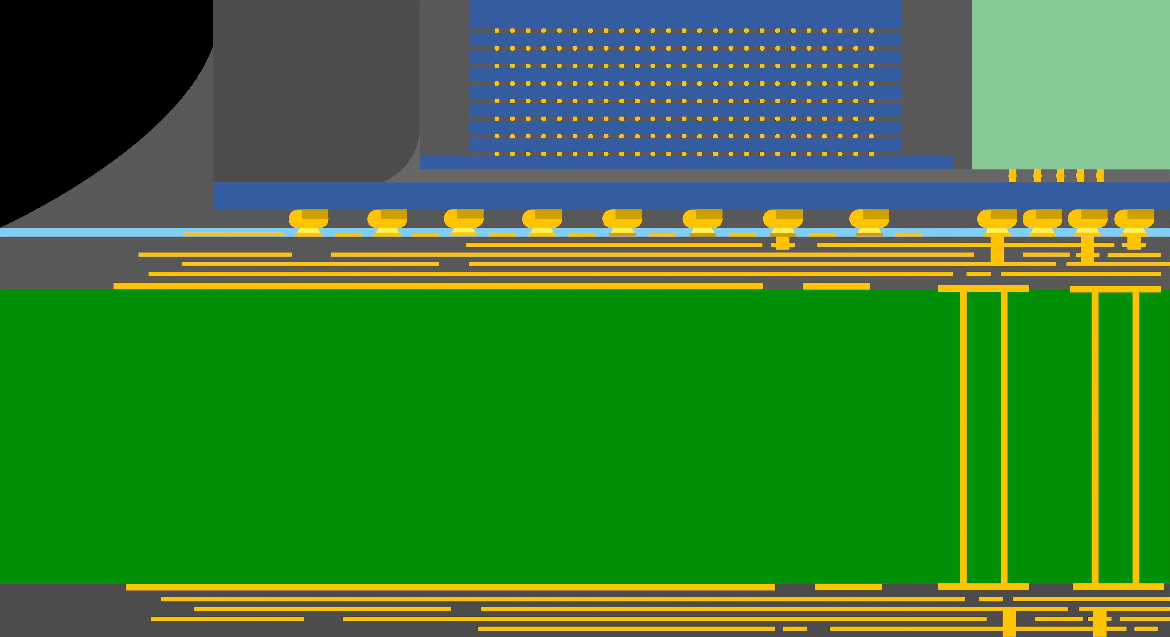
This is the deep asymmetry of open AI silicon: it is most achievable precisely where the money isn't. At the edge — inference on mature nodes, ordinary memory, no exotic packaging — open designs already exist and ship. At the frontier, where a training chip must marry a half-billion-dollar design to sold-out memory, sold-out packaging, and a twenty-year software moat, "open" barely gets a foot in the door.
The politics track the money. When Washington barred NVIDIA's most powerful chips from China — a saga that ran through the H100 ban and the on-again, off-again fate of the cut-down H20 — Beijing's answer was a push into domestic AI accelerators: Huawei's Ascend and Cambricon's MLU line. But these make a revealing counterpoint. They are home-grown and sanction-resistant, yet resolutely proprietary, built on in-house architectures rather than open ones; Huawei has open-sourced only its CUDA-rival software toolkit, never the silicon. Domestic is not the same as open. Europe, characteristically, is trying to be both: the European Processor Initiative fitted its accelerator with a RISC-V "tensor tile" for machine learning, and its 2025 successor program, DARE, is funding sovereign AI inference chiplets across the continent — open at the ISA, European-controlled at the design. Meanwhile the hyperscalers simply buy the talent, absorbing RISC-V AI startups like Rivos and Ventana into Meta and Qualcomm — a subject the ledger returns to below.
So the AI accelerator is where the insurgency has advanced furthest and stalled hardest at once. The open ISA has become the default vocabulary of AI compute — even NVIDIA and Google salt their own chips with RISC-V cores. The open-software stacks are landing real blows on the CUDA moat. And at the edge, open accelerators are fabricated and shipping. But the frontier — the training silicon on which the entire trillion-dollar AI economy actually runs — remains the least open corner of computing, walled off not by any instruction set but by memory, money, and software. The insurgency has reached the gates of the empire's richest city. It has not taken it.
Democratizing the fab
An open blueprint is worthless if turning it into physical silicon still costs millions. The deeper revolution — the one that put chip design within a student's reach — happened when the tools went free.
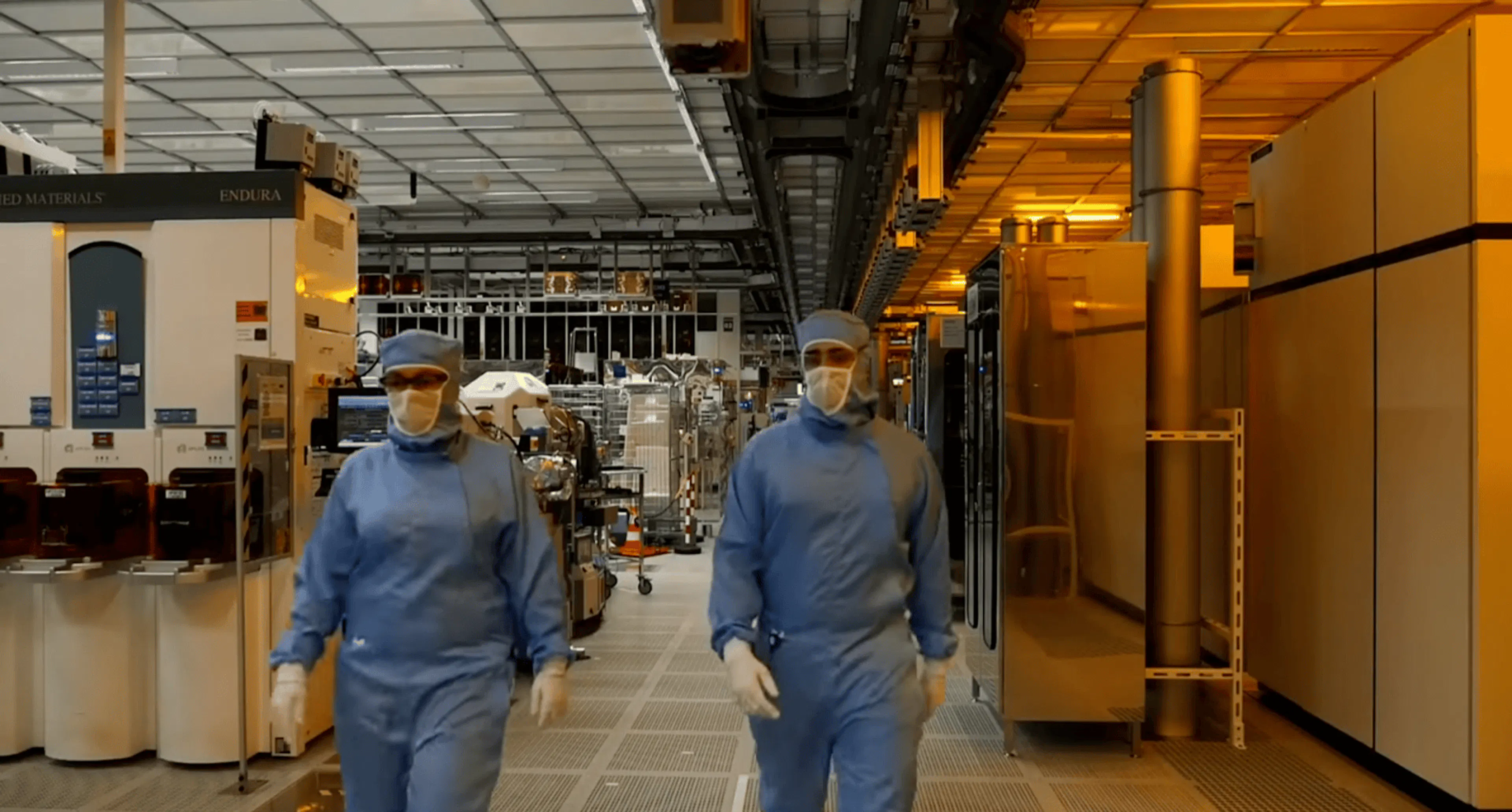
Translating hardware code into a physical layout once demanded proprietary Electronic Design Automation software from giants like Synopsys and Cadence, at millions a year. The DARPA-backed OpenROAD project shattered that barrier, delivering a fully autonomous "no-human-in-the-loop" flow that turns a design into a tapeout-ready layout in under 24 hours. Paired with the synthesis tool Yosys and the OpenLane/LibreLane flow, it has now been used in over 600 tapeouts.
The missing piece was the Process Design Kit — the foundry's secret recipe book for a given manufacturing process. In 2020, Google and SkyWater Technology released the first fully open, manufacturable PDK (a 130nm process), later joined by a GlobalFoundries 180nm node. For the first time in history, you could go from a keyboard to real, working silicon with zero proprietary software and no NDA. To make it affordable, projects like Tiny Tapeout packed hundreds of independent designs onto a single shared wafer, dropping the cost of a physical, packaged chip to a few hundred dollars.
The crash that proved the model
Then, in March 2025, the ecosystem got a brutal lesson in fragility. Efabless — the commercial platform that aggregated open designs and brokered access to foundries for the whole community — abruptly shut down after failing to secure new funding, stranding Tiny Tapeout projects inside the SkyWater fab and triggering a crisis of confidence.
What happened next is the real story. Rather than collapse, the community distributed its risk. By the end of 2025, new pathways had emerged: ChipFoundry stepped in to provide access to the SkyWater process and its own shuttle runs; Wafer.Space revived access to the GlobalFoundries node; and a coalition of European initiatives funded a port of the Tiny Tapeout infrastructure to a state-of-the-art 130nm process known for some of the world's fastest high-frequency transistors. The Efabless collapse, painful as it was, forced the movement to mature from dependence on a single sponsor into a resilient, multi-foundry network — coordinated, fittingly, over open chat protocols.
Hardening the core
Perhaps the most striking validation of open silicon comes from the hyperscalers using it to fix security problems that proprietary black boxes never could.
For decades, the cryptographic Root of Trust — the foundational chip that verifies a device's boot sequence and guards its firmware — was an opaque component you simply had to trust not to contain flaws or backdoors. The OpenTitan project, governed by the nonprofit lowRISC and backed by Google, Western Digital, Nuvoton, and ETH Zürich, built the world's first open-source silicon Root of Trust, applying commercial-grade verification — over 90% functional coverage across tens of thousands of nightly tests — to a design anyone can inspect.
In a milestone moment in 2026, OpenTitan chips, manufactured by Nuvoton, began shipping commercially inside enterprise Dell Chromebooks, securing the devices' firmware from the ground up. Crucially, OpenTitan is the first commercial Root of Trust to support post-quantum secure boot, meaning device firmware stays verifiable even if a future quantum computer cracks today's encryption. Its sibling, Caliptra — driven by AMD, Nvidia, Microsoft, and Google under the Linux Foundation's CHIPS Alliance — does the same job for the high-value chips inside data centers, ensuring only cryptographically signed firmware can run on a server's components.
Then there is CHERI. Roughly 70% of all serious software vulnerabilities trace back to memory bugs — buffer overflows, use-after-free errors — the kind that have plagued C and C++ for half a century. The University of Cambridge's CHERI project attacks the problem in hardware, extending the RISC-V ISA so that every memory pointer carries cryptographically protected bounds and permissions, guarded by an unforgeable hardware tag. Reach even one byte outside the permitted region, and the hardware traps the instruction instantly — fine-grained safety at near-zero performance cost. The approach is already commercializing: chip-IP vendor Codasip has shipped a RISC-V core with CHERI instructions, letting developers recompile legacy C/C++ into memory-safe binaries without rewriting it.
You cannot audit a black box for a backdoor. You can read open RTL line by line. For governments and security-critical buyers, that difference is becoming decisive — with the sober caveat that open source code is not the same as a verified physical chip, and the foundry itself remains a boundary of trust.
The main event: silicon as sovereignty
Everything to this point has been prologue to the reason open silicon is now discussed in capitals rather than just in labs. The logic is brutally simple: the United States can add a company to an export blacklist, but it cannot blacklist a standard. RISC-V International deliberately relocated its incorporation to Switzerland in 2020, explicitly to insulate the standard from U.S.–China trade tensions. It is the one layer of the entire computing stack outside Washington's direct reach.
China and the immune architecture
When U.S. export controls cut Huawei off from ARM and advanced chips starting in 2019, China embraced RISC-V as a strategic hedge — and the move has paid off in scale: China now accounts for roughly half of global RISC-V chip shipments. In 2025, eight government bodies issued the country's first national-level guidance promoting RISC-V adoption. The technical spearheads are Alibaba's T-Head unit (the XuanTie cores) and the Chinese Academy of Sciences (XiangShan); in March 2025, Alibaba unveiled the server-grade XuanTie C930, with a 16-stage pipeline and 6-wide decode.
American lawmakers have noticed. In late 2023, a bipartisan group — including the House Select Committee on the CCP and Senators Rubio and Warner — urged the Commerce Department to scrutinize how China uses RISC-V to "circumvent U.S. dominance" of chip-design IP. The dilemma is genuine and unresolved: any control broad enough to slow China would also hamstring U.S. firms — Google, Nvidia, Qualcomm, and Intel are all major RISC-V members — and would be nearly unenforceable against an open standard. No broad RISC-V restriction has been enacted.
But here is the catch that keeps Beijing's strategists awake: designing a sanction-proof chip is only half the battle. Manufacturing an advanced one still depends on TSMC, or on the lithography machines built by the Dutch company ASML — and those are very much export-controlled. The architecture is immune. The factory is not.
Europe's strategic autonomy
Europe frames RISC-V as essential to its "strategic autonomy" from both Washington and Beijing. The European Processor Initiative built the EPAC accelerator around RISC-V vector tiles, fabricated on GlobalFoundries' technology, targeting high-performance and scientific computing. Its successor program, DARE (Digital Autonomy with RISC-V in Europe), launched in March 2025 with EuroHPC backing — 38 partners across 13 countries, coordinated by the Barcelona Supercomputing Center — to build the processors, vector accelerators, and AI units for Europe's exascale supercomputers.
India's self-reliance
India has staked out the same ground under its Digital India RISC-V (DIR-V) program, part of the broader Atmanirbhar Bharat (self-reliance) drive. IIT Madras developed the SHAKTI family of open RISC-V processors, from tiny embedded cores to server-class designs, guaranteeing the country a domestic supply immune to global shocks. And the academic work has spun out commercial ventures: Mindgrove Technologies recently launched the S2401 "Secure IoT," billed as India's first indigenously designed high-performance microcontroller — fabricated on TSMC's 28nm node at 700 MHz, undercutting equivalent Western chips by around 30% while baking in hardware security. State-sponsored sovereignty, in other words, translating directly into market competitiveness.
The business of free
There is an obvious paradox in building an industry on something free: you can't sell what anyone can copy. The money, accordingly, is made not on the ISA but on implementations, IP, and services — and the sums have grown serious.
SiFive, founded by RISC-V's Berkeley creators, is the bellwether; an oversubscribed funding round announced in April 2026 valued it at $3.65 billion, with Nvidia among the investors, even as it pivots hard toward data-center AI. By its own account, its IP appears in more than 500 designs, with over 10 billion cores shipped to date. Tenstorrent, Jim Keller's company, closed a round in late 2024 at a roughly $2.6 billion valuation, with Bezos Expeditions, Hyundai, and Samsung among its backers. Consolidation has begun: Qualcomm acquired the data-center RISC-V startup Ventana Micro Systems in December 2025, and Meta acquired the AI-chip startup Rivos in 2025 — both signals that the giants want RISC-V expertise in-house.
Market forecasts, tellingly, diverge wildly — a hallmark of an immature field. One firm pegged the RISC-V SoC market at $6.1 billion in 2023, growing toward roughly $90 billion by 2030; the analysts at Omdia project shipments climbing nearly 50% a year to 17 billion processors by 2030, capturing almost a quarter of the global market. The numbers should be read as directional, not precise. The unifying theme is explosive unit growth, driven by IoT, automotive, and AI.
The honest bottom line
Strip away the breathless framing and the picture is clear-eyed and, in its own way, more impressive for being real.
Open-source silicon has decisively won the embedded and microcontroller world, where it is already cheaper and just as good. It has reached genuine parity with mid-range data-center cores at the level of published designs like XiangShan, even as commodity RISC-V hardware still trails the best of Intel, AMD, Apple, and ARM by roughly a CPU generation in raw single-thread speed. The open GPU remains years behind — a vital research platform, not yet a product. The open AI accelerator follows the same law of gravity: real and shipping at the low-power edge, a fertile research vanguard in the data center, but effectively locked out of the frontier, where the price of admission is sold-out memory, sold-out packaging, and a twenty-year software moat. And the whole stack now rests on a foundation of free design tools and open manufacturing recipes that simply did not exist a decade ago.
But the deepest shift is not measured in benchmarks. It is that the foundational vocabulary of computing is no longer owned. A standard governed in Switzerland, extensible by anyone, embargoable by no one, has become the instrument through which China, India, and Europe each pursue technological sovereignty — and against which Washington's most powerful tool, the export blacklist, simply does not bite.
The era in which a handful of companies dictated how the world's software speaks to the world's hardware is ending. What replaces it is messier, slower in places, and far harder to control. Which is, of course, precisely the point.
Sources & further reading
- RISC-V standard and governance: RISC-V — Wikipedia; Center for Security and Emerging Technology — "RISC-V: What it is and Why it Matters".
- XiangShan: Hot Chips 2024 slides on Kunminghu; RISC-V Summit Europe 2025 — Prof. Yungang Bao on Kunminghu V2.
- Tenstorrent / Ascalon: Tenstorrent RISC-V CPU page; "The Open Hardware Revolution"; EE Times — "Tenstorrent Productizes RISC-V CPU and AI IP".
- Shipping RISC-V hardware: Milk-V Pioneer; Tom's Hardware — SG2042 for HPC; DeepComputing MuseBook; SpacemiT V100 server chip.
- Western Digital SweRV and the embedded quiet empire: Western Digital press release; OpenHW Group CORE-V family on GitHub.
- Open GPUs: Vortex on GitHub; "Vortex: OpenCL Compatible RISC-V GPGPU"; RV64X — Design And Reuse; Libre-SOC; Kazan.
- AI accelerators — canonical designs and open vanguard: Kung & Leiserson, "Systolic Arrays," 1978; Jouppi et al., "In-Datacenter Performance Analysis of a Tensor Processing Unit," ISCA 2017; NVDLA Primer; Gemmini on GitHub; PULP Platform paper (2024); Columbia ESP.
- Tenstorrent Blackhole and Esperanto: Tenstorrent Blackhole; tt-metal on GitHub; ServeTheHome — Esperanto ET-SoC-1; Ainekko acquisition of Esperanto IP.
- The CUDA moat and open counter-stacks: Computer Weekly — "CUDA at 20"; Triton on GitHub; OpenXLA — Google Open Source Blog; Qualcomm acquires Modular.
- Fabrication democratized: SkyWater SKY130 open PDK; Zero to ASIC — post-Efabless recovery; Tom's Hardware — Efabless shutdown.
- Security — OpenTitan, Caliptra, CHERI: Google Open Source Blog — "OpenTitan shipping in production"; lowRISC — OpenTitan ships in Chromebooks; Caliptra — Google Cloud Blog; CHERI — Wikipedia; Codasip CHERI page.
- Sovereignty and geopolitics: European Processor Initiative — Wikipedia; The Register on DARE; SHAKTI processor — Wikipedia; Mindgrove S2401 Secure IoT.
- The two walls — HBM, packaging, and cost: Gholami et al., "AI and Memory Wall," IEEE Micro 2024; SemiAnalysis — CoWoS and HBM Supply Chain; McKinsey — chip design costs by node; SK Hynix Q3 record — CNBC.
- Consolidation: Meta acquires Rivos — Next Platform; Qualcomm acquires Ventana.
Image credits: all photographs and illustrations sourced from Wikimedia Commons and reproduced here under their respective licenses (CC BY-SA, CC BY, CC0, or public domain) for editorial illustration. Individual credits appear in each caption.
如有侵权请联系:admin#unsafe.sh